Modifying a CH341A For SPI Write Blocking and Forensics
IoT Forensics
Practical
DFIR
Jan 15, 2026
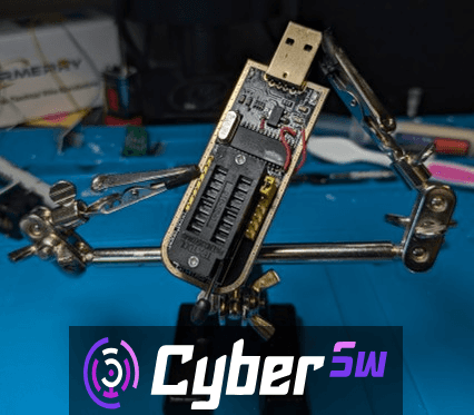
Modifying a CH341A For SPI Write Blocking and Forensics
Write blocking is a core part of digital forensic analysis, however the equipment to protect individual flash chips against writes at the hardware level does not exist for some forensic laboratories. Those that do exist are not sold at a price point that is attainable for small labs or for private training for professionals at home. The aim with this project was to show that it is possible to create hardware writeblockers for forensic analysis of IoT devices at home, easily, on a budget, with off the shelf parts.
This write blocker will work with the most common flash chips found inside of small consumer IoT devices that use the Serial Peripheral Interface (SPI). SPI is an interface used for inter-chip communication and is often the interface used between small flash chips (512KB-2GB) and system on chips (SoCs) inside of embedded systems. These chips are also found inside of laptops and PCs and usually contain the UEFI/BIOS and firmware. This write blocker could also be used in a forensic analysis of that lower level code if it was suspected to be modified.
How it Works
Much like a USB flash drive or SATA drive, there isn’t one specific pin that is used to write to the storage media of an SPI flash chip. Instead there are instructions that are sent to the chip by the interface for reading, writing, or deleting data, the address where the operation should take place and finally any data to be written. This means that write blocking isn’t as simple as disconnecting a pin prior to imaging.
The way that most write blockers work for other interfaces is by intercepting those instructions then inspecting them for any write commands before sending them to the media. One advantage that we have with SPI chips is that they have a standard write protect pin (WP) built into the specification. If this pin is grounded or “pulled low”, the chip performs the logic that most write blockers will do and reject any inbound write commands.
All this means to the forensic investigator on a budget is that all you have to do to make a write blocker that works with most SPI chips, is disconnect the WP pin from power (VCC), and connect it to ground. One thing to keep in mind with this modification is that it will not work on every single SPI chip. While the standard pinout has the WP pin, some newer and higher capacity chips utilize the pin in this position for an additional data line or other auxiliary features. In these instances data can still be written to the chip with this modification. Always make sure to check the target chip’s data sheet before running it in the reader as it may not have this feature. Other chips might have other considerations such as needing additional logic level shifting so always remember to check your datasheets before imaging.
At the same time, we are also going to perform a very common modification of our chip reader to allow it to operate at a lower voltage to add an additional layer of protection to our chips. Running the chips at the stock five volts is ok for short periods of time and hobby projects, but for forensic analysis, we want to ensure that the physical media stays intact so we are going to reduce the operating logic level to 3 volts.
How to Make Your Own
Everything that I did:
Bog standard voltage mod
Lift chip leg
Mask pad
Measure wire from point to point
Cut n strip
Solder in both wires
Clean
Initial design for the write blocking mod
Cut the 3.3v line to the WP pin
Short the WP pin to ground
Implement the write blocking mod
Test to make sure that the thing was still recognized by the computer
Find out I missed a line 3.3V line so I was actually just shorting 3.3V to ground (BAD).
Figure out what line it was
Desolder the socket
Trace tracing
Resolder
Cut said line
Re-route 3.3v to the 3.3v rail
Clean
Test
It was recognized and data lines were at 3.3v!
Test on SPI chip to make sure it still read stuff
It read!
Unfortunately I did not have a WPable chip so check datasheets
Tools and Materials
Required:
Gloves
Fume Extractor
Soldering iron with a small tip
Solder wick
Tweezers
Wire Strippers
Hoby Knife
Multimeter
Isopyopyl Alcohol
Cotton Swabs
Leaded Solder
Kapton tape
30 AWG wire or smaller
A computer or VM with USB passthrough running Linux
The flashrom package
I would recommend Debian or a Debian or Ubuntu based distribution like Kali Linux, Tsurugi Linux, or Attify OS
A test SPI chip with a WP pin
Recommended Optional Tools:
Helping Hands
Magnifying glass
Microscope
Tutorial
Before you start, ensure that you have your fume extractor turned on, gloves on, and all of your tools ready and available to you. Remember, when soldering to always work in a well ventilated room and to wash your hands after you are completed. Lead is nasty but the negative effects of working incorrectly with it are cumulative and long term so take the time to be safe.
The first part of the build is to change the operating voltage of the programmer to protect chips that operate at this lower voltage. There are a few different ways to do this but I used this method described in the flashrom documentation as it was what I found to be what worked on my programmer. All of these methods will route 3V to pin 28 of the CH341A chip instead of the 5V it is currently receiving.
Start by applying flux to the ping shown, then heating the pin with your soldering iron set to 400°C while applying a little bit of fresh solder. This will make desoldering the pin easier.
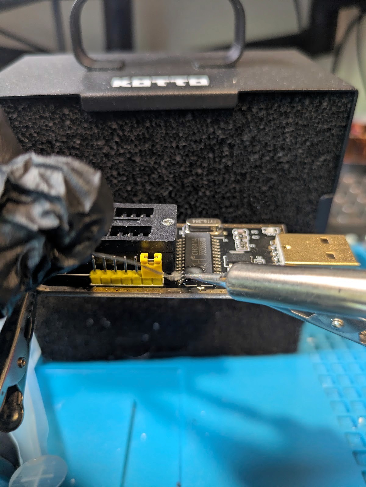
Figure 1: Adding solder to the VCC pin of the CH341A chip
Now with your tweezers, apply light pressure on the bottom of this pin while heating it with the soldering iron.
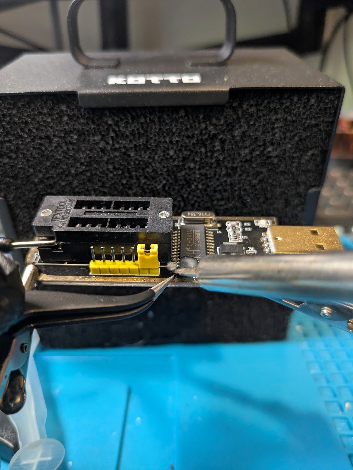
Figure 2: Lifting the VCC pin of the CH341A chip on the interface board
Once the pin is lifted, use the solder wick to clean up any additional solder left on the pin and the pad it was once connected to.
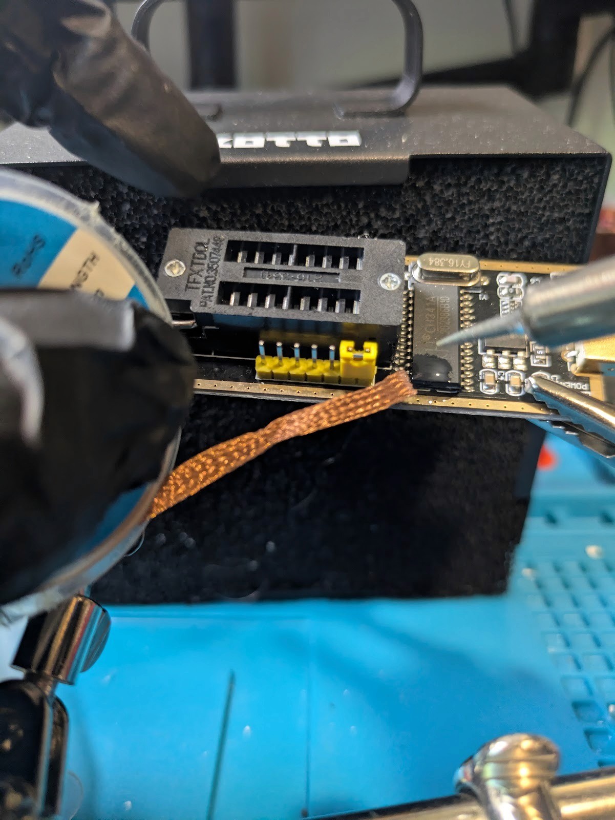
FIgure 3: Removing excess solder from the VCC pin of the CH341A chip
Now clean up the area with a little bit of isopropyl alcohol and a cotton swab to ensure that there isn’t any remaining flux.
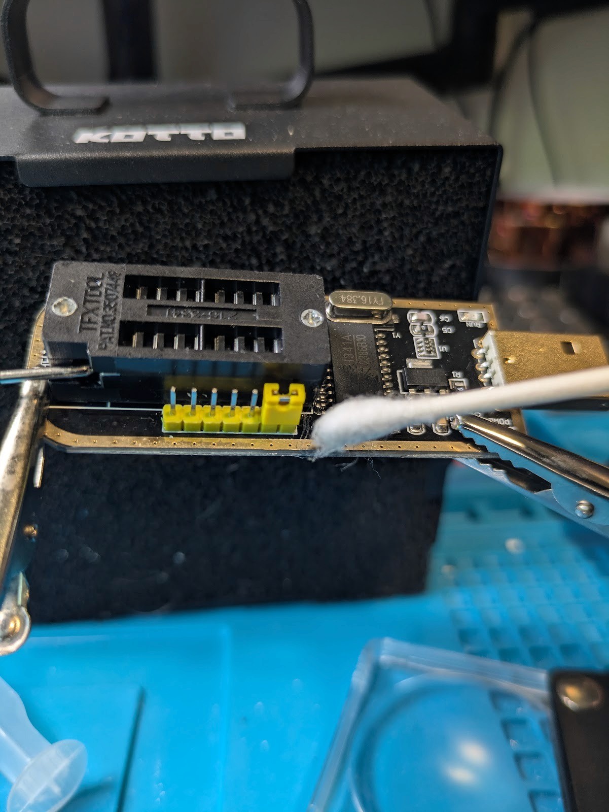
Figure 4: Cleaning the CH341A interface with a cotton swab and isopropyl alcohol after desoldering the VCC pin
Once the alcohol has evaporated, apply a small strip of kapton tape to the pin below to ensure that there aren’t any short circuits with this pin.
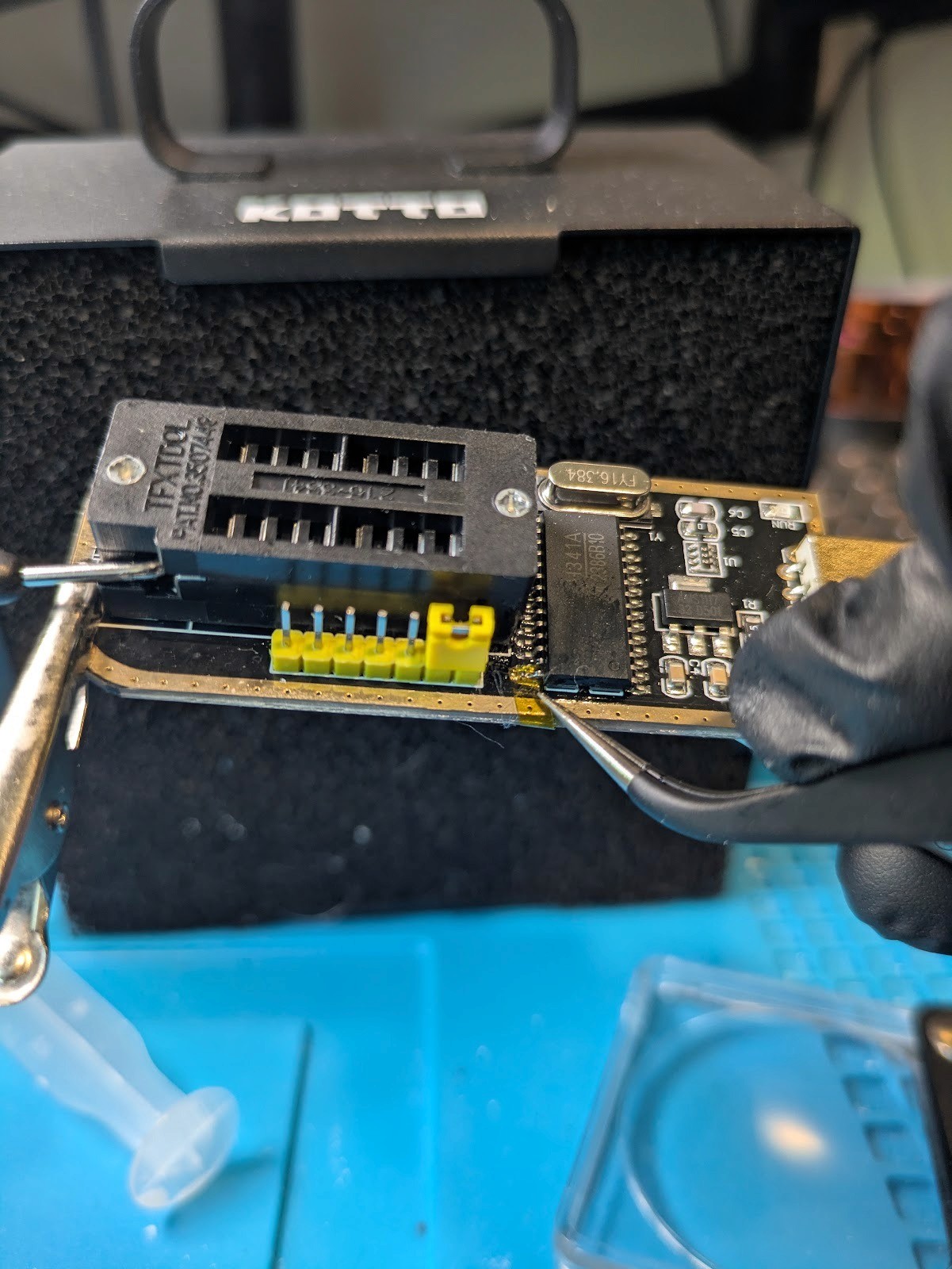
Figure 5: Applying a small amount of kapton tape underneath the VCC pin of the CH341A chip
Now, measure, cut, and strip a small length of wire to run between this pin and the 3V supply that is on the upper side of the C4 capacitor. Use a felt pen to mark the wire and cut a few millimeters more than you think you will need.
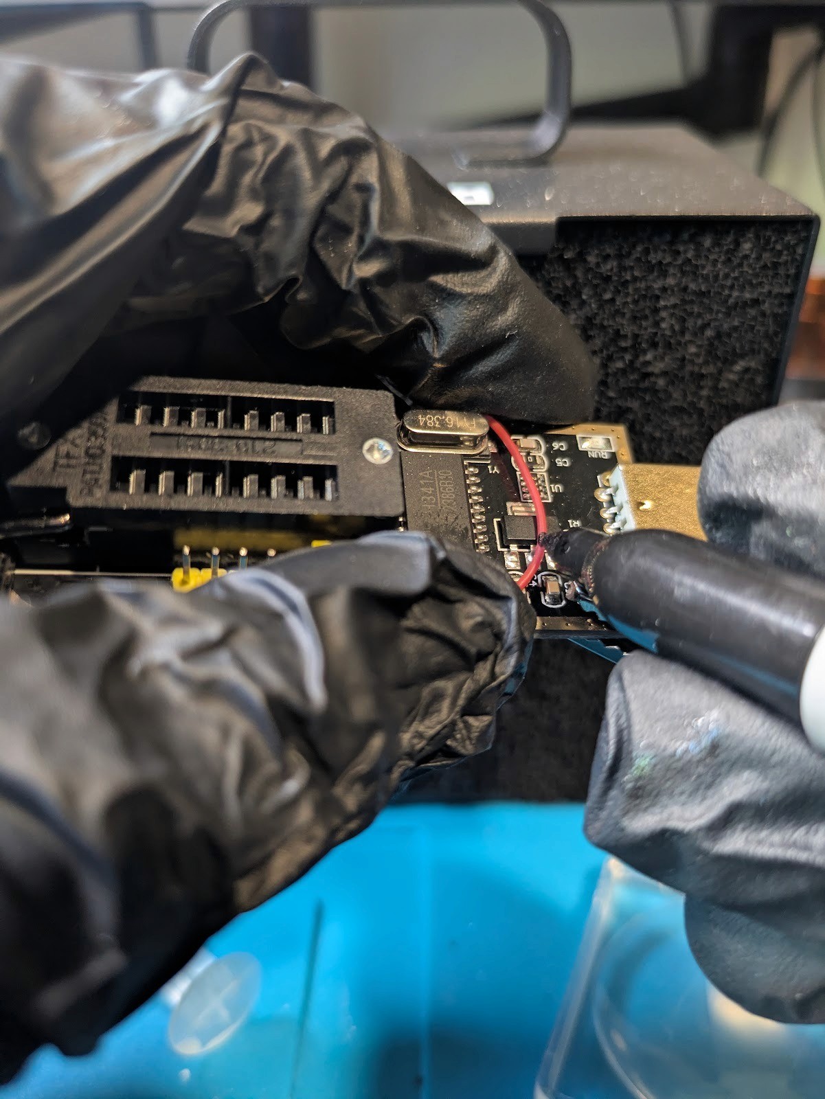
Figure 6: Measuring a length of wire to go between the C4 capacitor and the VCC pin on the CH341A interface
This wire to both C4 and the pin that was lifted earlier, then clean with isopropyl alcohol.
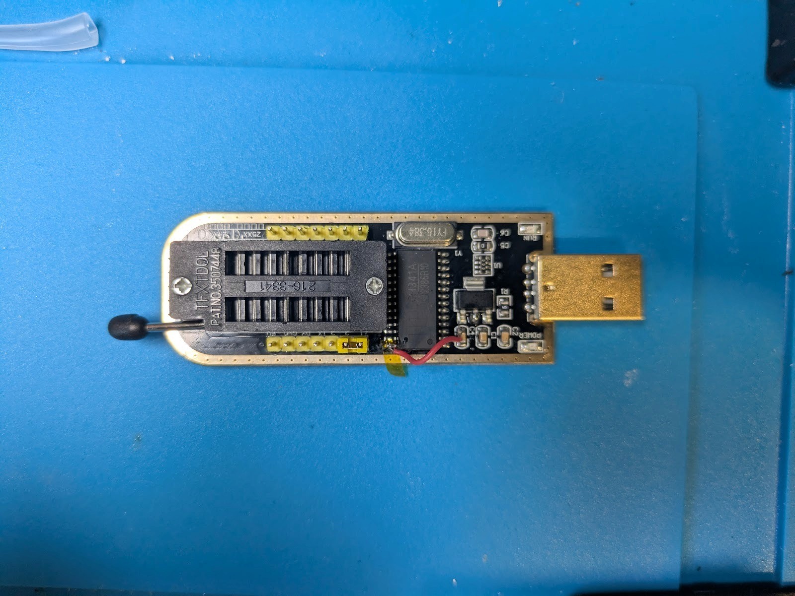
Figure 7: The completed connection between the VCC pin and C4 capacitor.
Next solder a small wire between the large pin on the 3V regulator and pin 9 of the CH341A chip and clean with isopropyl alcohol again. Ensure with each of these small connections that there is no solder bridging between any points that you create and surrounding components.
Figure 8: The fully modified CH341A interface with the additional connection between the large pin of the 3V regulator and pin 9 of the CH341A chip outlined in red.
At this point, it is wise to test your programmer before continuing. First check for shorts between any of the points that you soldered and any pins that are close by with a multimeter. Plug in the adapter. If there isn't a light on the board, then there is a good chance that you may have shorted VCC to ground and you should unplug the board immediately. Test that all of the data pins are reading between 3V and 3.3V. If everything looks good try connecting a chip and reading it with flashrom.
In my case, the only test chips that I have are running at 1.8V so I have to use the step down adapter before connecting it to the chip adapter. One thing to note about these adapters is that they should still work with the stepped down voltage but it is always important to check the datasheets of the voltage regulators that they use before using them to make sure they will still work with a lower input voltage than the stock 5V.
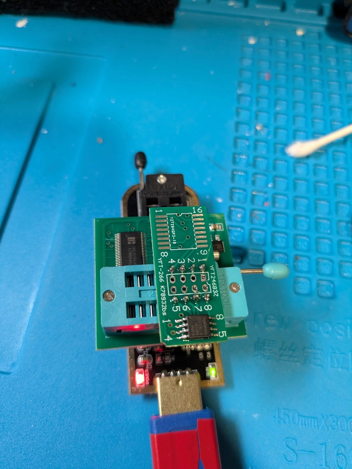
Figure 9: Testing the voltage modded CH341A adapter. The additional boards attached to the chip are a 1.8v logic level converter on the bottom and a breakout board with the chip soldered to it for ease of testing.
If you are using a VM, ensure that your CHA341A adapter is passed through to it before continuing. Open a terminal then run the following command to read the contents of the chip. This will take some time to complete but if you see that it detected the chip you can be very confident that it can read the whole chip.
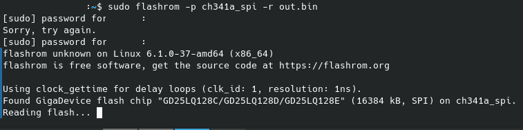
Figure 10: Imaging the SPI chip with the modified interface
Once that is done, you can inspect the contents of the file with your hex editor or firmware analysis tool of choice to see if the full contents were extracted.
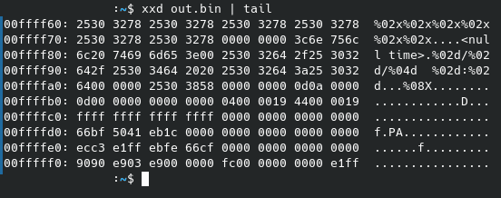
Figure 11: Displaying part of the contents of the image using the hex dump generator xxd
If you got all zeros or all F’s, it might be because your chip does not have any data on it. Try writing a short bit of data to the flash chip by creating a text file, then running ‘sudo flashrom -p ch341a_spi -w testfile.txt’ to write the data to the chip. Run the read command again and ensure that you could recover that data that you wrote to it.
If you still weren’t able to pull an image, really double check that all of the connections are solid between the chip and the adapter, then move towards the adapter, checking all of the solder connections that you made previously. Look for any solder bridging or stray wires that are connecting pins that shouldn’t be connected.
If everything worked, you can move on to implementing write protection on the adapter. This process involves scrapping away two traces that connect the WP pin to VCC and the other components that need that connection, reconnecting the parts that need VCC, then connecting WP to ground.
Start by locating the 3V traces on the board. This is more difficult because of the color of the PCB but if you catch the light just right you can see right through to the traces. The two places that need to be cut are highlighted in red and right next to the socket and pin that was previously lifted and on the underside of the board where it is connected to the rest of the pins that need 3V.
Figure 12: The fully modified CH341A with the location of the VCC trace that needs to be scratched away outlined in red.
Figure 13: The CH341A interface with the trace that needs to be scratched through highlighted in red.
Simply use a hobby knife to scrape away both the solder mask and the copper below. Do this in small increments to prevent going too far through. You want to stop just after the connection is broken and not any further.
To test that this worked, set your multimeter to continuity mode, then probe the WP pin against that 3V coming off of the voltage regulator that you soldered too earlier. If there wasn’t a connection you can mask off the exposed conductors with kapton tape.
Making these two cuts will disconnect a few other pins that need 3.3V from receiving it. To route power to the other pins, solder a wire to the outside pin of C1 on the other side of the board. Then solder the other side of that wire to the VCC or hold pin of the SPI socket. Ensure that there are no shorts, then plug in the adapter. If the VCC pin on the socket measures 3V continue to the next step.
Figure 14: The fully modified CH341A interface with the C1 capacitor outlined in red
Figure 15: The fully modified CH341A interface with the VCC pins that need to be connected to outlined in red.
The last thing that needs to happen is connecting the write protection pin to ground. This will signal the chip to not accept any write commands. There is a ground pin located right next to the write protect pin so all that needs to be done is to solder a small length of wire between these pins like so.
Figure 16: The fully modified CH341A interface with the pins that need to be bridged outlined in red
Finally, test the adapter again just like you did before. This time when you write the chip, you shouldn’t be able to! If you were still able to write to the chip, make sure that your chip supports writeblocking by checking its datasheet.
Conclusion
While it isn’t perfect, this is the best rudimentary option on a budget of >$20 to learn about forensic imaging of SPI chips. Ideally, a forensic writeblocker should be intercepting all signals between the interface and the chip and blocking any write instructions or even just an interface with no capabilities of writing to the chip. If you would like to learn more about how the protocol works on the wire, this could be done with an arduino and a little bit of programming to decode the signals to detect any write signals.

Frequently asked questions
Still have questions?
Can’t find the answer you’re looking for? Please chat with our friendly team.